Categories
-
Electronics 303
-
Food processing machines 3435
- Bakery - Coating, paning and breading machines 68
- Bakery - dough dividers, moulders and sheeting machines 111
- Bakery - kneading machines 161
- Bakery - other machines 61
- Beaters / mixers / tumblers 269
- Brine injection machines 21
- Butchery - Bowl Cutters 40
- Butchery - cutters / slicers / choppers / portioning machines 333
- Butchery - mincers / grinders 130
- Butchery - slaughterhouses 14
- Butchery - stuffers 128
- Candy / Sweets machines - miscellaneous machines 150
- Candy / Sweets machines - simple / double twist wrapper 62
- Candy / sweets machines - cutting and wrapping machines 70
- Chocolate machines 181
- Coating pans 37
- Coffee roasters 115
- Complete biscuit or croissant production lines 61
- Complete bread production lines 38
- Complete pasta or pizza production lines 37
- Cookers 81
- Dairy - butter production, wrapping and portioning machines 24
- Dairy - cheese production, wrapping and portioning machines 58
- Dairy - cream separators 31
- Fryers 53
- Miscellaneous (food) 385
- Ovens - cooking tunnels 51
- Ovens - multi-deck / stoves / rotary ovens 72
- Pasteurisers 46
- Refrigeration - cold rooms / cold stores 47
- Refrigeration - cooling tunnels 58
- Refrigeration - ice cream machines 40
- Skinning / filleting machines 138
- Smokehouses 20
- Vegetable and fruit cutting, washing and blanching machines 172
- Wine, beer or alcohol making machines 71
-
Metal - Presses/ Forging 1042
-
Metal - machine tools 8937
- Bar feeders 73
- Borers - deep hole boring / drilling machines 42
- Borers - floor type boring machines 30
- Borers - floor type boring machines CNC 63
- Borers - table type boring machines 132
- Borers - table type boring machines CNC 128
- Broaching machines 24
- Drilling - automatic/ CNC turret drilling machines 21
- Drilling - floor type drilling machines (column, pillar) 20
- Drilling - others (multispindle, column, pillar...) 35
- Drilling - radial drilling machines 97
- Edm - die sinking machines 140
- Edm - wire cutting machines 189
- Finishing - lapping / honing / deburring machines 77
- Finishing - others (washing / tumbling / vibratory...) 26
- Gear machines - others (milling, testing, inspection..) 34
- Gear grinding machines 33
- Gear hobbing cnc machines 49
- Gear hobbing manual machines 51
- Gear shaping machines 49
- Grinding machines - cylindrical centerless grinders 114
- Grinding machines - cylindrical external / internal grinders 304
- Grinding machines - miscellaneous (crankshaft, sharpening, tool grinders ...) 179
- Grinding machines - surface grinders 302
- Lathes - 0 - 3000 mm 383
- Lathes - > 3001 mm - heavy duty lathes 216
- Lathes - Multispindle automatic lathes 304
- Lathes - Swiss type lathes 72
- Lathes - cnc lathes 1267
- Lathes - others 24
- Lathes - vertical turret lathes 62
- Lathes - vertical turret lathes with cnc 151
- Machining centers - 5 axis 363
- Machining centers - high-speed (18000+ rpm) 49
- Machining centers - horizontal 290
- Machining centers - palletized 126
- Machining centers - vertical 1284
- Milling - travelling column milling machines 72
- Milling - universal milling machines 299
- Milling - cnc bed type milling machines 316
- Milling - cnc universal milling machines 229
- Milling - miscellaneous machines 73
- Milling - portal / gantry milling machines 136
- Others 470
- Planing machines 13
- Rotary transfers 22
- Saws for metal - band saws 257
- Saws for metal - others (hacksaws, slitting saws, circular...) 126
- Shaping - vertical / horizontal shaping / slotting machines 41
- Spring machines - multislide / formers / coilers 25
- Thread rolling machines 49
-
Metal - sheet metal machines 3655
- Combining machines laser / punch 21
- Complete unwinding units 10
- Cutting machines - Laser 516
- Cutting machines - Plasma / gas 243
- Cutting machines - Waterjet 58
- Deburring machines 23
- Folding machines 59
- Leveling / straightening machines 60
- Notching machines 28
- Others sheetmetal machinery 133
- Plate rolling machines 140
- Plate rolling machines - 4 rolls 125
- Press brakes 227
- Press brakes cnc/nc 629
- Profile bending machines 119
- Punching machines / nibbling machines 96
- Punching machines / nibbling machines with CNC 263
- Shears - hydraulic guillotines 287
- Shears - mechanical guillotines 40
- Shears / guillotines CNC 155
- Slitting lines / Cut to length lines 58
- Tube bending machines 154
- Welding machines 149
- Welding positioners 59
-
Miscellaneous industrial equipment 2796
- Complete units 88
- Compressed-air plants 13
- Compressors 122
- Conveyors 109
- Cranes - Bridge cranes / hoisters 76
- Cranes - Tower cranes - gantry 20
- Dehydration and filtering 81
- Electricity - Generator sets 159
- Energy 30
- Forklifts - Diesel forklifts 18
- Forklifts - Electric forklifts 39
- Forklifts - Gas forklifts 8
- Glass machinery - Cutting - Edging 70
- Glass working machines - Bevelling 12
- Glass working machines - Insulating 27
- Glass working machines - Miscellaneous 80
- Glass working machines - washing - coating - printing 22
- Heat / surface treatment 40
- Industrial boilers 108
- Industrial ovens 92
- Liquids cooling 178
- Measure - controls - Miscellaneous 40
- Measure - controls - Profile projectors 22
- Measuring units 144
- Miscellaneous 532
- Miscellaneous Handling - Lifting 70
- Pallet racks - storage units - Kardex 17
- Public works - Miscellaneous 10
- Pumps and industrial pumping systems 65
- Robots - ABB 83
- Robots - Fanuc 43
- Robots - Kuka 117
- Robots - Others 81
- Robots - Staubli 12
- Spray booths / painting units 64
- Stone industry equipment - marble and granite 42
- Vacuum cleaning units 45
-
Packaging - conditioning 5281
- Bagging machines - Horizontal - Flowpacks 271
- Bagging machines - Vertical - Sachet machines 235
- Baling presses - waste compactors 11
- Blister machines 200
- Bundlers 48
- Capping machines - cappers - crimping machines 253
- Cartoning machines / cartoners - Horizontal 276
- Cartoning machines / cartoners - Vertical 123
- Case packers 194
- Cellophane / overwrapping machines 144
- Checkweighers 183
- Feeders - scales - sorting machines 229
- Filling machines - Bottling equipment 211
- Filling machines - Food industry 144
- Filling machines - Tube fillers 326
- Filling machines - Various equipment 166
- Filling machines - Vials / ampoules fillers 91
- Inspection machines 71
- Labellers 642
- Metal detectors 105
- Miscellaneous packaging machines 204
- Multihead weighers 79
- Palletizers - palletizing robots 52
- Shrink wrap machines / Sealers 216
- Shrinking tunnels 52
- Strapping machines 28
- Stretch wrapping machines 104
- Taping machines 26
- Tea / Coffee bag machines 38
- Thermoforming - Form, Fill and Seal, FFS lines 367
- Tray sealers 186
-
Pharmaceutical - Chemical 3336
- Mills 223
- Miscellaneous pharmaceutical / chemical machines 241
- Mixers - Multishaft and Planetary Mixers 569
- Mixers / Blenders - Powder solid 165
- Mixers / Homogenizers - Liquid cream 220
- Pharmacy / medical - complete production lines 60
- Tablet coating machines 54
- Tablet presses - rotary / rotary compacting presses 179
- Tablet presses - single-punch / eccentric / single station press 106
- Tanks - boilers - melting tanks 372
-
Plastic - rubber 2567
-
Printing machines 2414
- 3D Printer 58
- Binding - gang stitchers / sewing machines 26
- Binding - gatherers / collators 79
- Binding - perfect binders / thermal binders 90
- Binding - saddle stitchers 91
- CTP computer to plate 71
- Carton and board converting machines 32
- Case making machines 25
- Die-cutters / Embossers / Hot foil 119
- Digital printing presses 224
- Envelopes - Insertion / Printing 63
- Flexo printing machines 67
- Folders - gluers / staplers / wire binders 214
- Label printing machines 133
- Laminators 80
- Letterpresses - cylinders / platens 13
- Offsets 1 colour 19
- Offsets 2 colours 54
- Offsets 4 colours 73
- Offsets 5 colours 55
- Offsets 6 colours 11
- Offsets 8 colours and more 28
- Others - post press machines 101
- Others - press and printing 119
- Paper and board machines - Others 43
- Paper and board machines - Sheeters / cut size 23
- Paper and board machines - Winders / rewinders / unwinders / slitters 65
- Plotters - Large format inkjet 151
- Screen printing equipment 77
- Trimmers - Guillotines / Cutters 130
- Trimmers - Three knife 15
- Web continuous printing presses 56
-
Textile machines 1140
- Complete plants/production units 32
- Cutting - automated cutting machines 138
- Cutting - spreading machines 21
- Embroidery machines - large orders embroidery machines 18
- Embroidery machines - one head / multi-heads 81
- Finishing - Washing / Steaming / Ironing machines / Folding machines 51
- Finishing - dryers 23
- Finishing - dyeing machines 52
- Finishing - stenters 8
- Knitting - circular knitting machines 67
- Knitting - flat knitting machines 82
- Knitting - knitting machines for socks / tights 46
- Miscellaneous used textile machines 94
- Printing - calenders 23
- Printing - rotary textile printers 57
- Printing - textile presses 32
- Sewing machines / making - automatic machines 76
- Special textile machines - equipments for non weaved textile 78
- Special textile machines - unrolling & inspection machines 11
- Spinning - carding machines 13
- Spinning - preparation 13
- Spinning - spinning machines 24
- Spinning - twisting / assembling 22
- Spinning - winders 34
- Weaving - looms 10
- Weaving - looms with jacquard 9
- Weaving - sectional warping machines 10
- Weaving - warp sizing machines 6
-
Woodworking machines 1650
- Boring, drilling and dowel inserting machines 52
- Briquetting machines 10
- Brushing machines 20
- Drying - kilns, ovens 22
- Dust collectors / exhausters 27
- Edgebanders - double sided 26
- Edgebanders - single sided 132
- Finger Joint machines 16
- Gluing machines 22
- Guillotines for veneer 29
- Miscellaneous wood machinery 61
- Moulders - multihead 111
- Moulders - spindle moulding machines 22
- Planing machines / Jointers 32
- Routers 17
- Sanding - Wide belt sanders 127
- Sanding / grinding - others 25
- Saws - band saws 19
- Saws - cross-cut optimizing saws 39
- Saws - multi-blade saws 63
- Saws - other (mitre, cut off) 28
- Saws - panel saws 88
- Saws - sliding table saws 27
- Spraying machines 61
- Tenoning machines 43
- Tree-bark and tree-trunks processing machines 7
- Wood CNC machining centres 215
- Wood CNC machining centres - 5 Axis 41
- Wood CNC machining centres - Doors and windows 21
- Wood Presses 104
- Wood chipping machines 29
- Wood combined machines 13
- Wood lathes 16
- Wood milling machines 34
- Woodworks plant and complete wood units 47
 Polovodiče - Waferovací stroje
 Halbleiter - Waferausrüstung
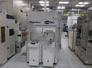
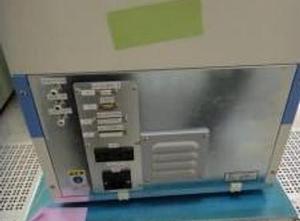
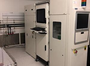
 Semiconductor - Wafer equipment
 Semiconductor - Equipo de wafer
 Semi-conducteur - Machines pour wafer
 Semiconduttori - Macchine per wafer
 Półprzewodniki - płytki (półprzewodnikowe)
 Полупроводники - Пластины
 Yarı İletken - Wafer Ekipmanları
 France

 Malaysia
 Ireland
 Hong Kong
 USA
USA